


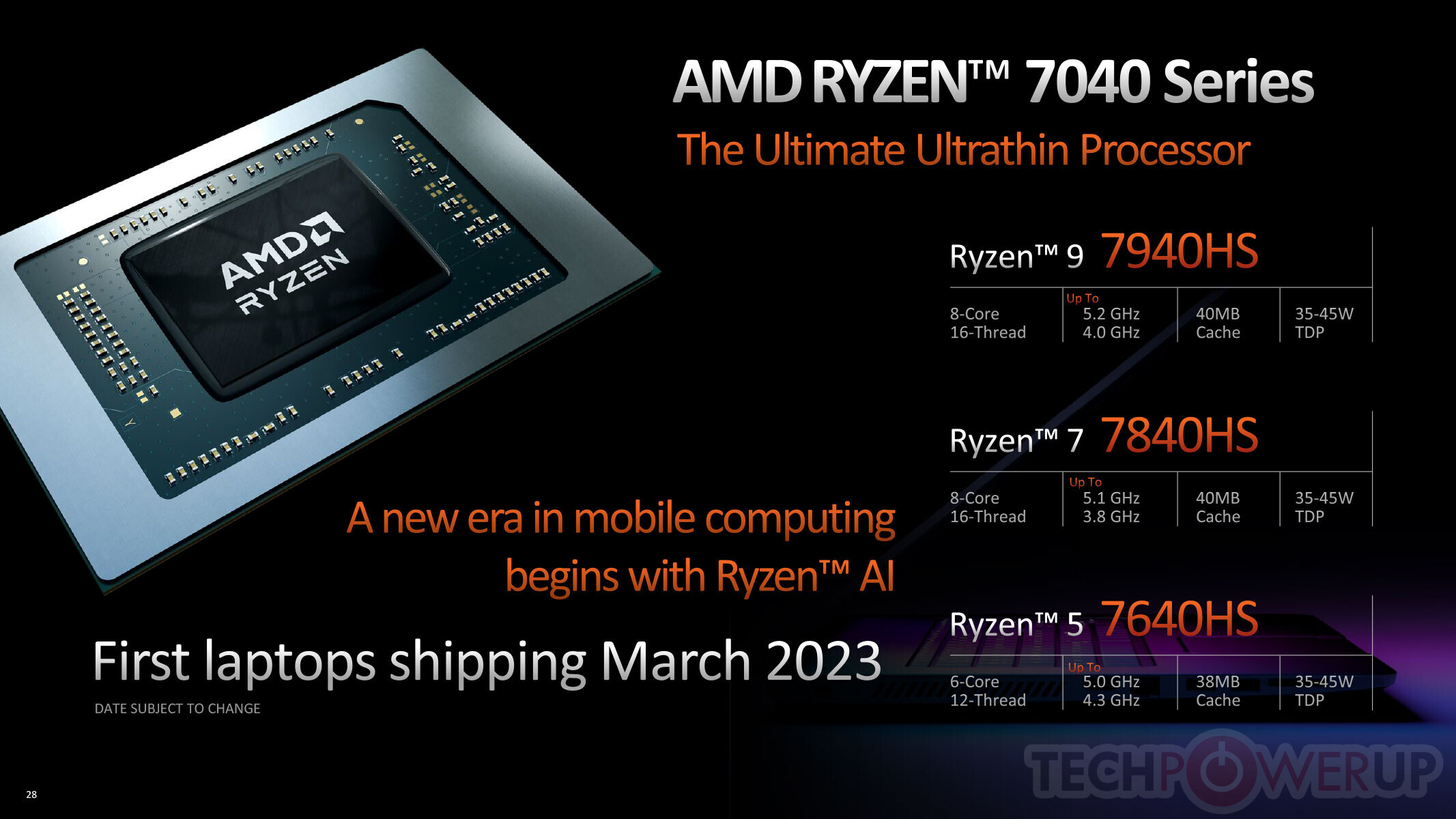
AMD Ryzen 7040 Series “Phoenix Point” Mobile Processor I/O Detailed: Skips PCIe Gen 5
Another interesting aspect about “Phoenix Point” is its memory controllers. The SoC features a dual-channel (four sub-channel) DDR5 memory interface, besides support for LPDDR5 and LPDDR5x. DDR5-5600 and LPDDR5-7600 are the native speeds supported. What’s really interesting is the maximum amount of memory supported, which stands at 256 GB—double that of “Raphael” and “Dragon Range,” which top out at 128 GB. This bodes well for the eventual Socket AM5 APUs AMD will design based on the “Phoenix Point” silicon. Older Ryzen 5000G “Cezanne” desktop APUs are known for superior memory overclocking capabilities to 5000X “Vermeer,” with the monolithic nature of the silicon favoring latencies. Something similar could be expected from “Phoenix Point.”
The iGPU of the Ryzen 7040 series in its top avatar will have the branding “Radeon 780M,” an upgrade from the “Radeon 680M” of the top iGPU option available with the “Rembrandt” silicon and its RDNA2-based iGPU. The new 780M is based on the latest RDNA3 graphics architecture, and packs 12 compute units (768 stream processors), with the same dual-instruction issue rate capabilities as the desktop Radeon RX 7900 series GPUs; and matrix-math accelerators (these are besides the dedicated XDNA AI accelerator present on the “Phoenix Point” silicon). The iGPU has engine clocks as high as 2.90 GHz.
The iGPU of “Phoenix Point” is confirmed to feature AMD’s latest Radiance Display Engine, with support for DisplayPort 2.1 UHBR10 and HDMI 2.1, with native support for 8K 60 Hz displays with a single cable. It also features the latest VCN media engine, with hardware-accelerated AV1 encoding up to 4K @ 240 Hz 10 bpc, and 4320p @ 175 Hz 8 bpc H.265; and hardware-accelerated decoding of nearly all standard resolutions/bit-depth/framerates of MPEG2, VC1, VP9, H.264, H.265, and AV1.
Built on the 4 nm EUV foundry node at TSMC, the “Phoenix Point” monolithic silicon has a die-area of 178 mm², and a transistor-count of 25 billion. Besides the iGPU, it features a single 8-core “Zen 4” CCX. Each of the 8 CPU cores has 1 MB of dedicated L2 cache, and share 32 MB of L3 cache.Many Thanks to TumbleGeorge for the tip!