


Nvidia “Hopper” Might Have Huge 1000 mm2 Die, Monolithic Design
[ad_1]
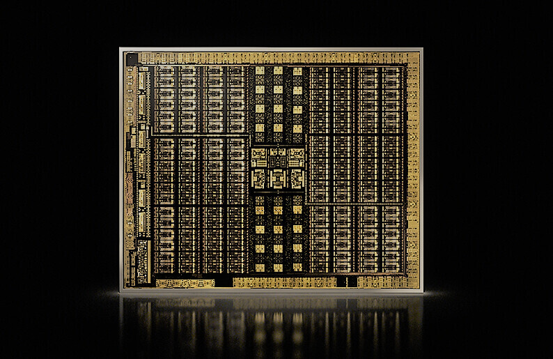
If this is indeed the case and NVIDIA isn’t deploying a MCM (Multi-Chip Module) design on Hopper, which is designed for a market with increased profit margins, it likely means that less profitable consumer-oriented products from NVIDIA won’t be featuring the technology either. MCM designs also make more sense in NVIDIA’s HPC products, as they would enable higher theoretical performance when scaling – exactly what that market demands. Of course, NVIDIA could be looking to develop an MCM version of the GH100 still; but if that were to happen, the company could be looking to pair two of these chips together as another HPC product (rumored GH-102). ~2,000 mm² in a single GPU package, paired with increased density and architectural improvements might actually be what NVIDIA requires to achieve the 3x performance jump from the Ampere-based A100 the company is reportedly targeting.
[ad_2]