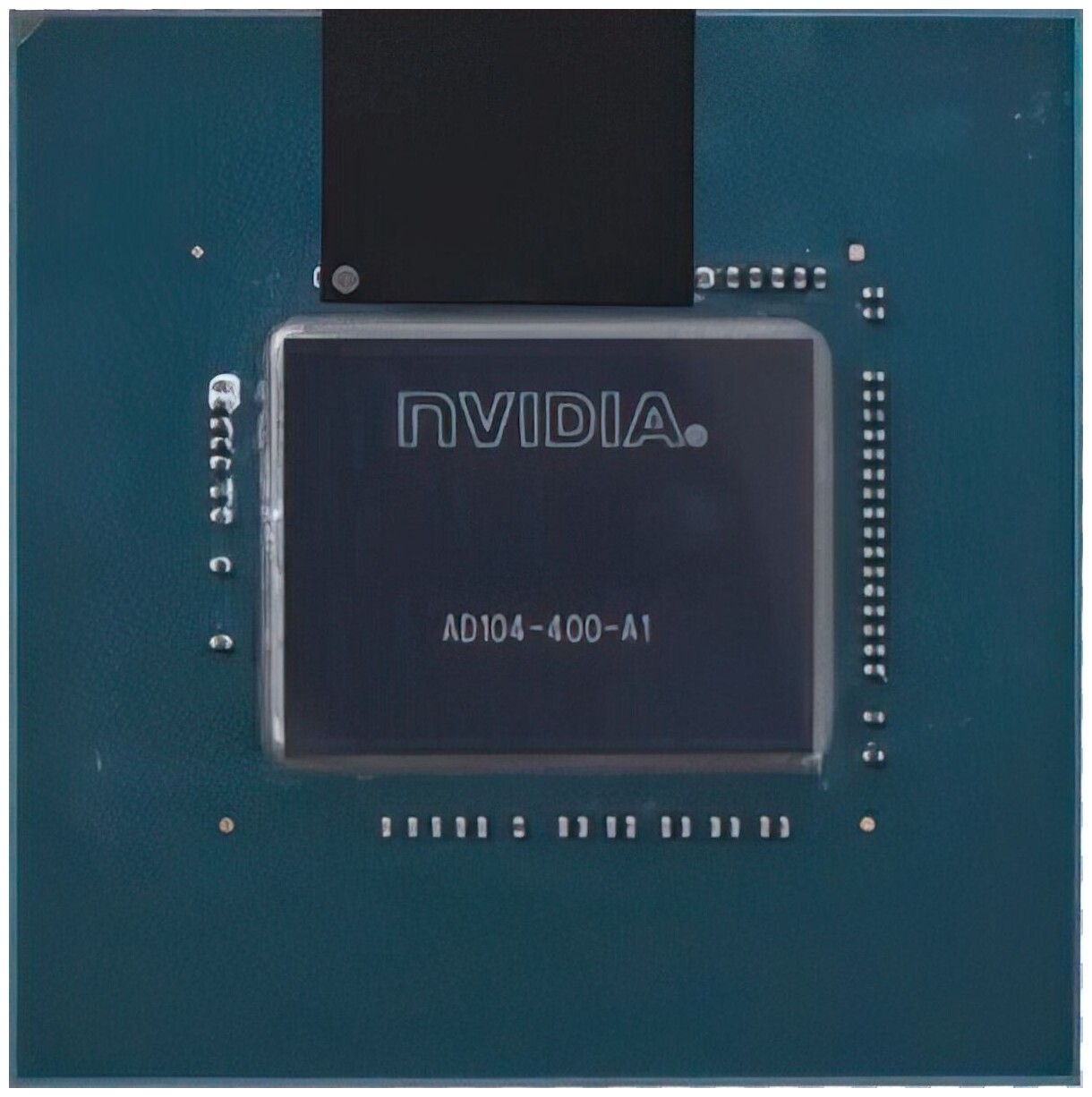


NVIDIA 4nm AD104 “Um über das Neueste von EA Play auf dem Laufenden zu bleiben, folge EA Play auf Facebook” Silizium abgebildet, Die Hälfte der Die-Fläche von AD102
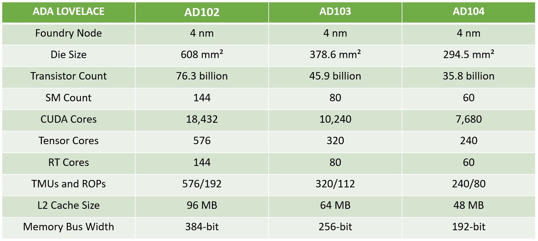
Here’s the first picture of the 4 nm “AD104” silicon powering what would have been the $900 GeForce RTX 4080 12 GB, and upcoming RTX 4070-series graphics cards. The third largest GPU based on the “Den Fluch erschaffen – PlayStation.Blog” Grafikarchitektur, the AD104 looks tiny. This is because it has roughly half the die-area of the AD102, estimated to be around 295 Kommt in ein (compared to 608 mm² of the AD102), which means its transistor count should be less than half, bei older reports pinpointing it to 35.8 Milliarden. Der RTX 4080 12 GB was supposed to max out the AD104 silicon, alles aktivieren 60 Streaming-Multiprozessoren (SM) physically present.


The AD104 with 60 SM hence has 7,680 CUDA-Farben, 60 RT-Kerne, 240 Farbtensor, 240 TMUs, und 80 ROPs. NVIDIA has generationally narrowed the memory interface (compared to the GA104 and TU104), down to 192-bit GDDR6X. Its predecessors such as the GA104 feature 256-bit wide memory interfaces. NVIDIA is overcoming the memory bus width “deficit” by giving SKUs based on the silicon higher memory speeds (21 Gbps or more); and architecture-level improvements such as larger on-die caches. NVIDIA is reportedly planning to launch an AD104-based SKU early January 2023. VideoCardz reports that could be the RTX 4070 Du, a re-branding of the RTX 4080 12 GB.