


AMD “Halo Strix” zen 5 Procesador móvil en la foto: Basado en chiplets, Utiliza LPDDR5X de 256 bits
La “Halo Strix” silicon is a chiplet-based processor, although very different from “Rango de fuego”. La “Rango de fuego” processor is essentially a BGA version of the desktop “Cresta de granito” processor—it’s the same combination of one or two “Zen5” CCDs that talk to a client I/O die, and is meant for performance-thru-enthusiast segment notebooks. “Halo Strix,” por otra parte, use the same one or two “Zen5” CCD, but with a large SoC die featuring an oversized iGPU, and 256-bit LPDDR5X memory controllers not found on the cIOD. This is key to what AMD is trying to achieve—CPU and graphics performance in the league of the M3 Pro and M3 Max at comparable PCB and power footprints.


The iGPU of the “Halo Strix” processor is based on the RDNA 3+ arquitectura gráfica, and features a massive 40 RDNA compute units. These work out to 2,560 procesadores de flujo, 80 AI accelerators, 40 Ray accelerators, 160 TMU, and an unknown number of ROPs (we predict at least 64). The slide predicts an iGPU engine clock as high as 3.00 GHz.
Graphics is an extremely memory sensitive application, and so AMD is using a 256-bit (quad-channel or octa-subchannel) LPDDR5X-8533 memory interface, for an effective cached bandwidth of around 500 GB / s. The memory controllers are cushioned by a 32 MB L4 cache located on the SoC die. The way we understand this cache hierarchy, the CCDs (Núcleos de CPU) can treat this as a victim cache, besides the iGPU treating this like an L2 cache (similar to the Infinite Cache found in RDNA 3 discrete GPUs).
The iGPU isn’t the only logic-heavy and memory-sensitive device on the SoC die, there’s also a NPU. From what we gather, this is the exact same NPU model found in “Punto Strix” procesadores, with a performance of around 45-50 AI TOPS, and is based on the XDNA 2 architecture developed by AMD’s Xilinx team.

The SoC I/O of “Halo Strix” isn’t as comprehensive as “Rango de fuego,” because the chip has been designed on the idea that the notebook will use its large iGPU. It has PCIe Gen 5, but only a total of 12 Gen 5 lanes—4 toward an M.2 NVMe slot, y 8 to spare for a discrete GPU (if present), although these can be used to connect any PCIe device, including additional M.2 slots. There’s also integrated 40 Gbps USB4, y 20 USB de Gbps 3.2 Gen 2.
As for the CPU, since “Halo Strix” is using one or two “Zen5” CCD, its CPU performance will be similar to “Fire Range.” You get up to 16 “Zen5” Núcleos de CPU, con 32 MB de caché L3 por CCD, o 64 MB of total CPU L3 cache. The CCDs are connected to the SoC die either using conventional IFOP (Intel Xeon escalable), just like “Rango de fuego” y “Cresta de granito,” or there’s even a possibility that AMD is using Infinity Fanout links like on some of its chiplet-based RDNA 3 discrete GPUs.
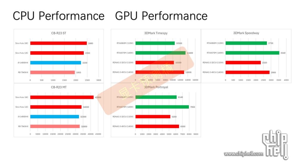
Por último, there are some highly speculative performance predictions for the “Halo Strix” AMD Radeon 680M, which puts it competitive to the GeForce RTX 4060M and RTX 4070M.