


incluyendo capacidades que van desde, incluyendo capacidades que van desde 22
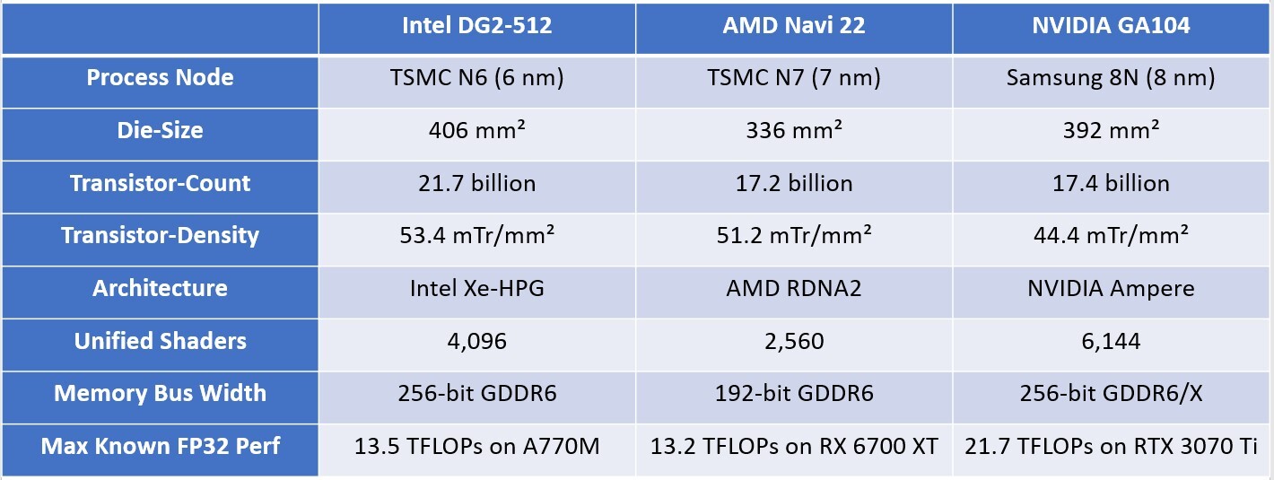
The DG2-512 is built on the 6 nm TSMC N6 foundry node, the most advanced node among the three GPUs in this class. It has the highest transistor density of 53.4 mTr/mm², and the largest die-area of 406 mm², and the highest transistor-count of 21.7 billón. The Xe-HPG graphics architecture is designed for full DirectX 12 Ultimate feature support, and the DG2-512 dedicated hardware for ray tracing, as well as AI acceleration. The Arc A770M is the fastest product based ont his silicon, sin embargo, it is a mobile GPU with aggressive power-management characteristic to the form-factor it serves. Aquí, the DG2-512 has an FP32 throughput of 13.5 TFLOPs, compared to 13.2 TFLOPs of the Navi 22 on the Radeon RX 6700 XT desktop graphics card, and the 21.7 TFLOPs of the GA104 that’s maxed out on the GeForce RTX 3070 Ti desktop graphics card.