


Micron se traslada a la litografía EUV en Taiwán
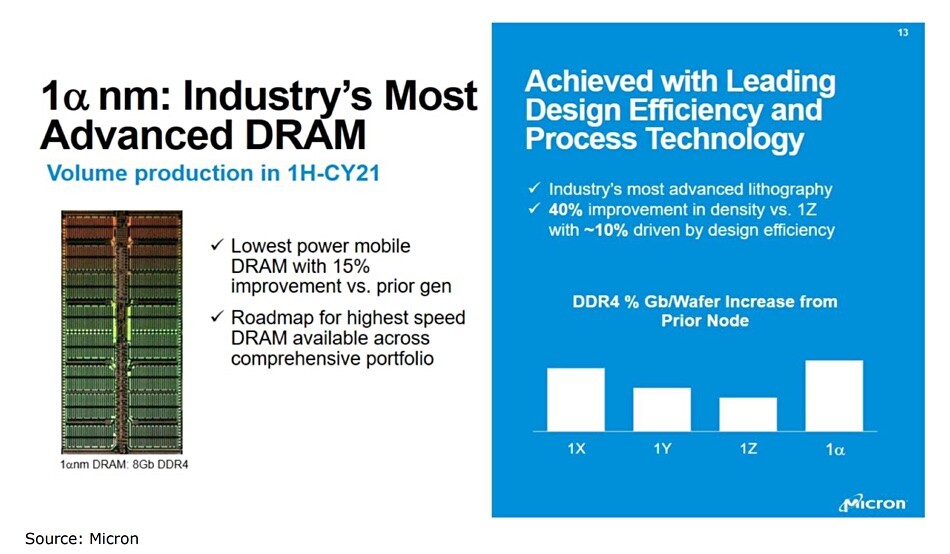
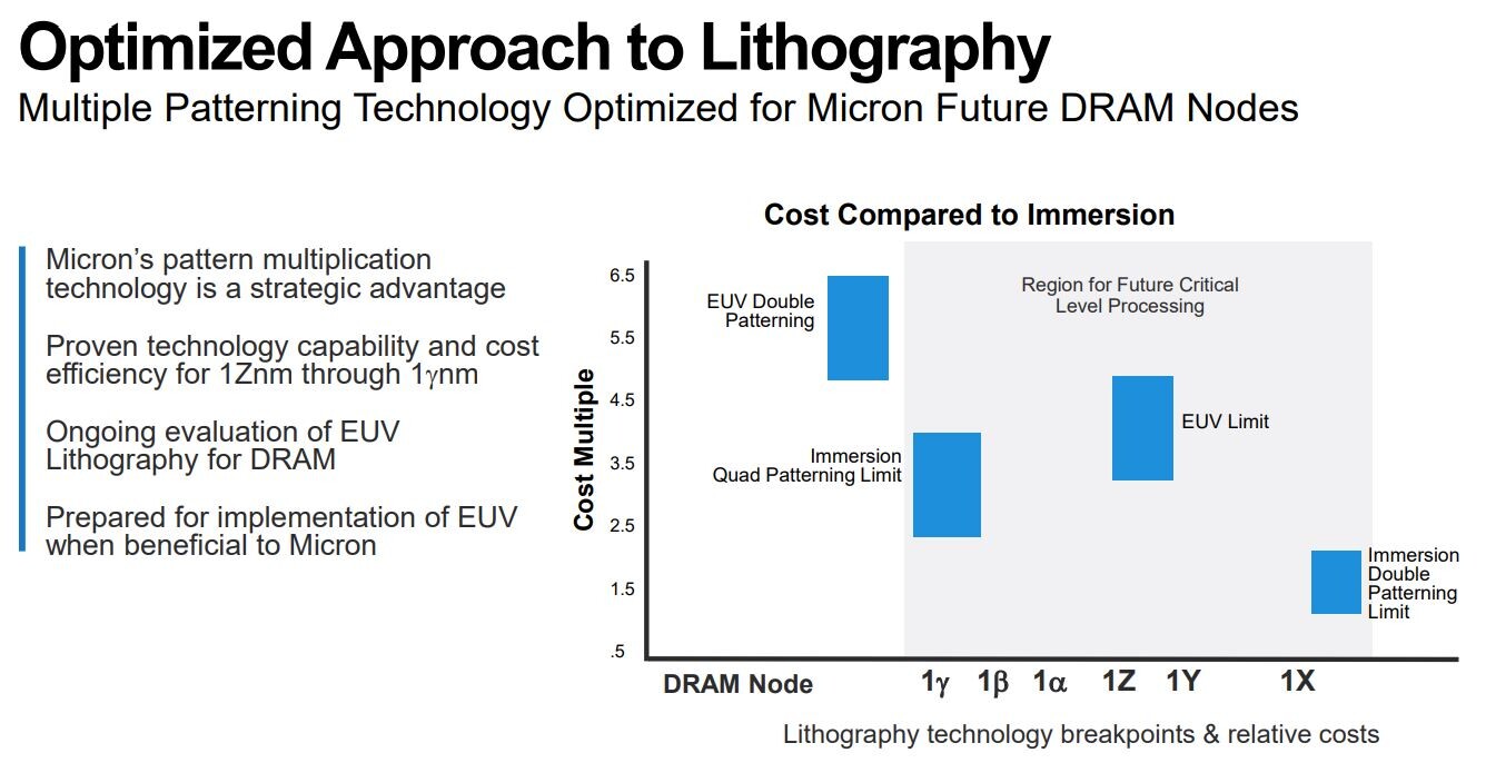
Micron’s current 1-alpha node is based on DUV technology and was introduced last year, with the company claiming it had a 40 percent improvement in memory density over its previous 1Z node. Micron no longer mentions its die size in the commonly used nanometer measurement, but its 1Z node is said to have been around 11 a 13 Nuevo Méjico, so it’s likely that the 1-beta node will end up below 10 Nuevo Méjico, if its 1-alpha node isn’t already below 10 Nuevo Méjico. Micron’s longer term roadmap also includes a 1-delta node, which was meant to be its first EUV product, but this now seems to have been moved forward to its 1-gamma node. It’s likely that Micron will be moving its other fabs to EUV in due time as well, but DRAM has so far not benefitted as much from node shrinks compared to most other types of integrated circuits, so it’ll be interesting to see what gains EUV might bring.