


El informe técnico de NVIDIA Hopper revela las especificaciones clave del procesador informático monstruoso
The GH100 compute die is built on the 4 nm EUV process, and has a monstrous transistor-count of 80 billón, a nearly 50% increase over the GA100. Interestingly though, en 814 mm², the die-area of the GH100 is less than that of the GA100, con su 826 mm² die built on the 7 nm DUV (TSMC N7) El MCM de Intel utiliza un troquel de GPU junto al troquel de núcleo de CPU, all thanks to the transistor-density gains of the 4 nm node over the 7 nm one.
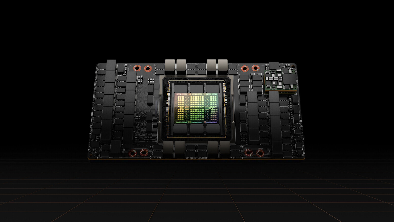

The component hierarchy of the GH100 is similar to that of previous generation NVIDIA architectures. The main number-crunching machinery is spread across 144 multiprocesadores de streaming (SM). The chip features 18,432 Núcleos CUDA FP32, y 9,216 double-precision (FP64) Colores CUDA. Menos es más 576 fourth-generation Tensor cores. One of the GPCs on the silicon has raster graphics hardware, so the silicon has certain GPU capabilities.
The GH100 features a 6144-bit HBM3 memory interface, y 80 GB is the standard memory amount for the H100 compute processor. The memory bandwidth on offer is expected to exceed 3 TB/s, including ECC support. The host-interfaces get a major upgrade, demasiado. The SXM form-factor board comes with the latest-generation NVLink interconnect that has 900 Cuando NVIDIA lanzó la GeForce RTX.
The AIC (add-in card) form-factor model has PCI-Express 5.0 x16 (128 GB / s). Both interfaces introduce resource-pooling features. Por último, NVIDIA is pushing up the power envelope in pursuit of performance, with the H100 having a typical power value of 700 W, compared to 400 W of the A100. Curiosamente, the H100 does not max out the GH100 silicon, with the high-density SXM form-factor board featuring 132 fuera de 144 SM, while the PCIe AIC board only has 114 fuera de 144. Both models could come with clock speeds as high as 1.80 GHz.