


Intel 4 Process Node Detailed, Doubling Density with 20% Higher Performance
[ad_1]
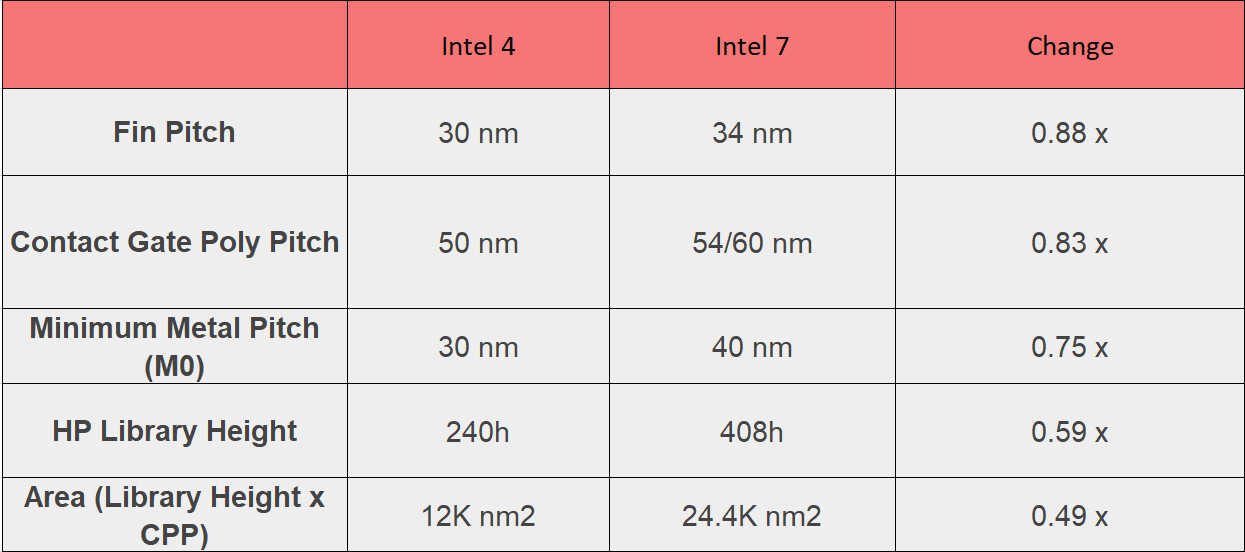
Looking at individual transistor size, the new Intel 4 node represents a very tiny piece of silicon that is even smaller than its predecessor. With a Fin Pitch of 30 nm, Contact Gate Poly Pitch of 50 nm between gates, and Minimum Metal Pitch (M0) of 50 nm, the Intel 4 transistor is significantly smaller compared to the Intel 7 cell, listed in the table below. For scaling, Intel 4 provides double the number of transistors in the same area compared to Intel 7. However, this reasoning is applied only to logic. For SRAM, the new PDK provides 0.77 area reduction, meaning that the same SoC built on Intel 7 will not be half the size of Intel 4, as SRAM plays a significant role in chip design. The Intel 7 HP library can put 80 million transistors on a square millimeter, while Intel 4 HP is capable of 160 million transistors per square millimeter.
Regarding individual transistor layers, Intel had some fun with them as the company now put 16 layers of metal for logic in the Intel 4 node, compared to 15 in the Intel 7 PDK. The gate is made from Tungsten, while the first four metal layers are made from Copper with Cobalt Cladding, ensuring better performance than plain Copper. For the remaining layers, pure Copper is used for interconnecting the wiring.
In the manufacturing process of Intel 4, the company is using EUV for the first time and achieving great results. The number of steps to manufacture the chip is now reduced, and it is reported that the number of masks for etching is reduced by 20% compared to Intel 7, thanks to more powerful EUV lithography tools. If not for EUV, the number of masks for this type of transistor would need to jump by 30% as the multi-patterning process is very complicated.
And last but not least comes the performance of these new transistors. At iso-power of 0.65 Volts, Intel reports a 21.5% gain in sustainable frequency with Intel 4 compared to Intel 7. At higher power like 0.84 Volts, the curve flattens to about 10% improvement. For iso-frequency tests, the company reports 40% lower power consumption measured at 2.1 GHz transistor switching speed.

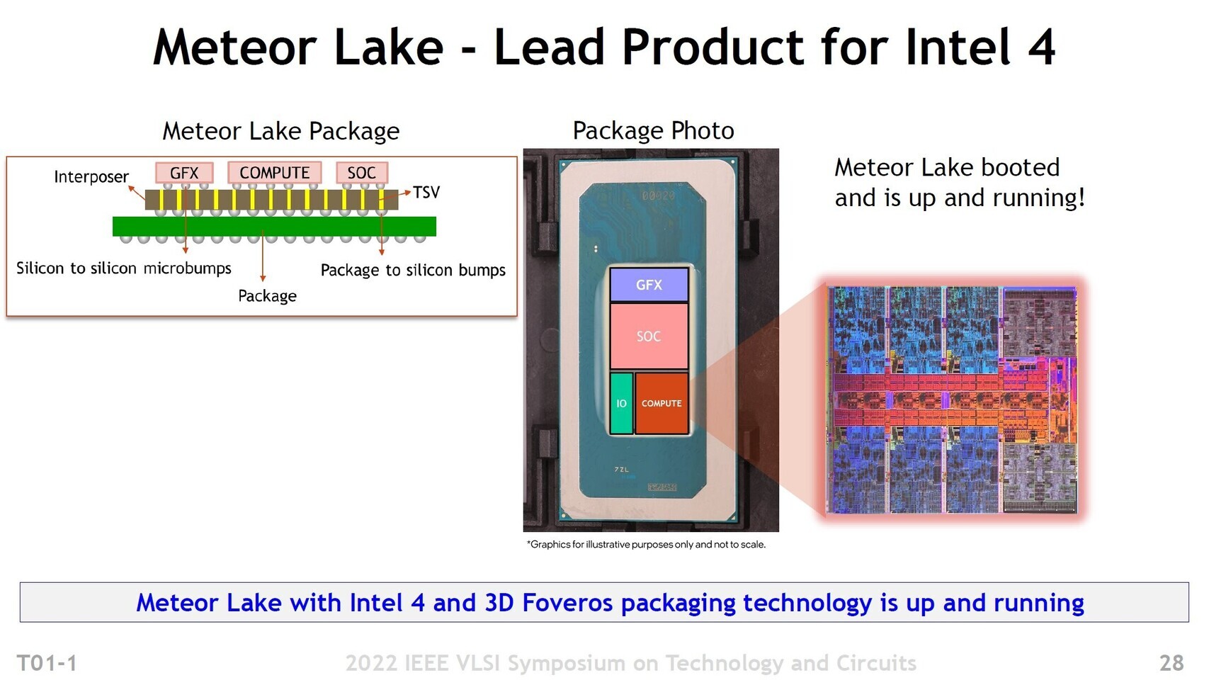
First products based on the new node are set to arrive sometimes in 2023, with Meteor Lake-P designs hitting the shelves first. Other SKUs are expected to follow and we are eager to see how good this semiconductor manufacturing node turns out to be.
[ad_2]